1. Product Characteristics and Structural Integrity
1.1 Innate Features of Silicon Carbide
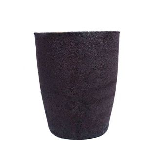
(Silicon Carbide Crucibles)
Silicon carbide (SiC) is a covalent ceramic compound made up of silicon and carbon atoms prepared in a tetrahedral lattice structure, mainly existing in over 250 polytypic types, with 6H, 4H, and 3C being the most highly pertinent.
Its strong directional bonding conveys exceptional hardness (Mohs ~ 9.5), high thermal conductivity (80– 120 W/(m · K )for pure single crystals), and impressive chemical inertness, making it one of the most durable products for extreme settings.
The vast bandgap (2.9– 3.3 eV) guarantees superb electrical insulation at room temperature level and high resistance to radiation damage, while its reduced thermal expansion coefficient (~ 4.0 × 10 ⁻⁶/ K) adds to remarkable thermal shock resistance.
These inherent buildings are preserved also at temperatures surpassing 1600 ° C, permitting SiC to keep architectural stability under extended direct exposure to thaw steels, slags, and reactive gases.
Unlike oxide ceramics such as alumina, SiC does not react conveniently with carbon or type low-melting eutectics in minimizing ambiences, an important advantage in metallurgical and semiconductor processing.
When fabricated into crucibles– vessels made to contain and heat products– SiC surpasses conventional products like quartz, graphite, and alumina in both life expectancy and process integrity.
1.2 Microstructure and Mechanical Security
The efficiency of SiC crucibles is carefully linked to their microstructure, which depends upon the production method and sintering additives utilized.
Refractory-grade crucibles are commonly created through reaction bonding, where permeable carbon preforms are penetrated with molten silicon, forming β-SiC through the reaction Si(l) + C(s) → SiC(s).
This procedure produces a composite framework of primary SiC with recurring complimentary silicon (5– 10%), which improves thermal conductivity but may restrict usage above 1414 ° C(the melting point of silicon).
Alternatively, fully sintered SiC crucibles are made through solid-state or liquid-phase sintering making use of boron and carbon or alumina-yttria ingredients, achieving near-theoretical density and higher pureness.
These display exceptional creep resistance and oxidation stability but are extra costly and tough to fabricate in plus sizes.
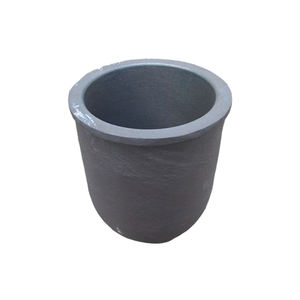
( Silicon Carbide Crucibles)
The fine-grained, interlacing microstructure of sintered SiC supplies exceptional resistance to thermal exhaustion and mechanical erosion, essential when handling molten silicon, germanium, or III-V substances in crystal growth processes.
Grain border engineering, consisting of the control of additional phases and porosity, plays an important function in determining long-lasting resilience under cyclic home heating and aggressive chemical environments.
2. Thermal Performance and Environmental Resistance
2.1 Thermal Conductivity and Heat Circulation
Among the defining benefits of SiC crucibles is their high thermal conductivity, which makes it possible for quick and uniform warmth transfer throughout high-temperature processing.
Unlike low-conductivity products like merged silica (1– 2 W/(m · K)), SiC successfully distributes thermal energy throughout the crucible wall, reducing localized hot spots and thermal slopes.
This uniformity is necessary in procedures such as directional solidification of multicrystalline silicon for photovoltaics, where temperature level homogeneity straight impacts crystal top quality and defect thickness.
The combination of high conductivity and low thermal growth causes a remarkably high thermal shock specification (R = k(1 − ν)α/ σ), making SiC crucibles resistant to fracturing during fast home heating or cooling down cycles.
This enables faster heater ramp prices, enhanced throughput, and reduced downtime due to crucible failure.
Moreover, the product’s capacity to hold up against repeated thermal biking without substantial deterioration makes it excellent for batch handling in commercial furnaces operating over 1500 ° C.
2.2 Oxidation and Chemical Compatibility
At elevated temperatures in air, SiC goes through passive oxidation, creating a protective layer of amorphous silica (SiO TWO) on its surface area: SiC + 3/2 O TWO → SiO TWO + CO.
This glazed layer densifies at heats, working as a diffusion barrier that reduces more oxidation and protects the underlying ceramic structure.
Nonetheless, in reducing atmospheres or vacuum conditions– typical in semiconductor and metal refining– oxidation is subdued, and SiC remains chemically stable versus molten silicon, light weight aluminum, and lots of slags.
It stands up to dissolution and reaction with molten silicon approximately 1410 ° C, although long term direct exposure can lead to slight carbon pickup or interface roughening.
Most importantly, SiC does not introduce metallic pollutants right into sensitive melts, an essential need for electronic-grade silicon manufacturing where contamination by Fe, Cu, or Cr must be kept listed below ppb degrees.
Nonetheless, treatment should be taken when processing alkaline earth metals or very responsive oxides, as some can corrode SiC at severe temperature levels.
3. Production Processes and Quality Control
3.1 Manufacture Strategies and Dimensional Control
The manufacturing of SiC crucibles involves shaping, drying out, and high-temperature sintering or seepage, with methods chosen based on required purity, size, and application.
Typical creating strategies consist of isostatic pushing, extrusion, and slip spreading, each supplying various levels of dimensional precision and microstructural uniformity.
For big crucibles utilized in photovoltaic ingot casting, isostatic pressing makes certain regular wall density and density, minimizing the risk of asymmetric thermal expansion and failing.
Reaction-bonded SiC (RBSC) crucibles are cost-efficient and extensively used in foundries and solar sectors, though recurring silicon limits maximum service temperature level.
Sintered SiC (SSiC) versions, while more costly, deal exceptional purity, strength, and resistance to chemical attack, making them ideal for high-value applications like GaAs or InP crystal development.
Accuracy machining after sintering might be required to achieve limited tolerances, especially for crucibles utilized in vertical gradient freeze (VGF) or Czochralski (CZ) systems.
Surface area completing is important to decrease nucleation websites for flaws and guarantee smooth thaw circulation during spreading.
3.2 Quality Control and Efficiency Validation
Rigorous quality control is essential to make sure reliability and long life of SiC crucibles under demanding functional problems.
Non-destructive examination methods such as ultrasonic screening and X-ray tomography are employed to spot inner fractures, gaps, or thickness variants.
Chemical evaluation through XRF or ICP-MS verifies low degrees of metal contaminations, while thermal conductivity and flexural toughness are gauged to validate material consistency.
Crucibles are frequently subjected to simulated thermal cycling tests before delivery to identify prospective failure settings.
Set traceability and qualification are common in semiconductor and aerospace supply chains, where component failure can bring about expensive production losses.
4. Applications and Technological Influence
4.1 Semiconductor and Photovoltaic Industries
Silicon carbide crucibles play an essential role in the manufacturing of high-purity silicon for both microelectronics and solar cells.
In directional solidification heaters for multicrystalline photovoltaic or pv ingots, huge SiC crucibles function as the main container for liquified silicon, sustaining temperature levels over 1500 ° C for several cycles.
Their chemical inertness prevents contamination, while their thermal stability makes certain uniform solidification fronts, causing higher-quality wafers with fewer dislocations and grain limits.
Some makers layer the internal surface area with silicon nitride or silica to additionally minimize bond and facilitate ingot release after cooling down.
In research-scale Czochralski growth of compound semiconductors, smaller sized SiC crucibles are made use of to hold melts of GaAs, InSb, or CdTe, where very little reactivity and dimensional stability are critical.
4.2 Metallurgy, Shop, and Arising Technologies
Beyond semiconductors, SiC crucibles are essential in metal refining, alloy preparation, and laboratory-scale melting operations including light weight aluminum, copper, and precious metals.
Their resistance to thermal shock and disintegration makes them optimal for induction and resistance heaters in factories, where they outlive graphite and alumina options by numerous cycles.
In additive manufacturing of responsive metals, SiC containers are used in vacuum induction melting to prevent crucible malfunction and contamination.
Arising applications consist of molten salt activators and focused solar power systems, where SiC vessels may consist of high-temperature salts or fluid steels for thermal energy storage space.
With ongoing breakthroughs in sintering innovation and layer engineering, SiC crucibles are positioned to sustain next-generation materials processing, making it possible for cleaner, much more effective, and scalable commercial thermal systems.
In summary, silicon carbide crucibles stand for an important allowing technology in high-temperature product synthesis, combining extraordinary thermal, mechanical, and chemical performance in a solitary engineered element.
Their prevalent fostering across semiconductor, solar, and metallurgical industries highlights their role as a keystone of contemporary commercial ceramics.
5. Provider
Advanced Ceramics founded on October 17, 2012, is a high-tech enterprise committed to the research and development, production, processing, sales and technical services of ceramic relative materials and products. Our products includes but not limited to Boron Carbide Ceramic Products, Boron Nitride Ceramic Products, Silicon Carbide Ceramic Products, Silicon Nitride Ceramic Products, Zirconium Dioxide Ceramic Products, etc. If you are interested, please feel free to contact us.
Tags: Silicon Carbide Crucibles, Silicon Carbide Ceramic, Silicon Carbide Ceramic Crucibles
All articles and pictures are from the Internet. If there are any copyright issues, please contact us in time to delete.
Inquiry us